
by Michael D’Agati
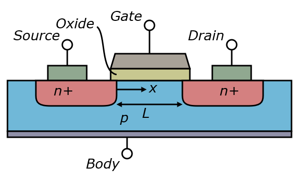
The number of transistors in an integrated circuit doubles every other year, according to Moore’s Law. This means that transistors must either continue to shrink beyond the nanoscopic scale or utilize different materials and geometries. However, limitations of atomic interactions at such a small scale make it difficult for transistors to be shrunk past the nanoscopic scale. In order to combat this conflict, new materials, such as graphene, and different device geometries are being employed in semiconductor devices. Graphene possesses special properties, including mechanical, electrical, and thermal attributes; the material’s charge carriers also have a very small effective mass, and its carrier mobility is upwards of 15,000 cm2/Vs.
Using graphene and an ultrathin ferroelectric film as a tunnel barrier, Shuoguo Yuan from The Hong Kong Polytechnic University and his colleagues recently created a vertical graphene-ferroelectric tunneling heterostructure (VGFTH). This type of transistor uses quantum tunneling. In other words, electrons pass through a barrier as the fundamental switching mechanism, instead of thermionic emission over a barrier. This allows for greater efficiency and power than a conventional metal-oxide semiconductor field effect transistor (MOSFET) of the same size. The VGFTH devices also save more power than standard metal-oxide semiconductor field effect transistors because they utilize a lower voltage.
The device in this article was produced using vapor deposition techniques (the material is deposited on the entire substrate and then etched away where it isn’t needed) on an oxidized silicon substrate. The graphene connected the source and the drain of the transistor, and BiFeO3 (BFO) was sandwiched between the graphene and drain, creating the ultrathin ferroelectric film. BFO was chosen as the ferroelectric film because of its small energy band gap and good polarization. This film allowed for an on/off current ratio of 7 x 10⁷, compared to the previously highest reported on/off ratio of 1 x 10⁶. Since this type of tunneling transistor has a small subthreshold swing (45 mV dec-1), the gate modulation ability was stronger, meaning less power consumption.
The results of this study provide an opening for a family of atomic-scale devices with 2-D layer building blocks. This new family would provide alternatives to the existing transistor technologies, allowing Moore’s Law to remain a reality. More studies with new materials and geometries like this will allow for the invention of future integrated circuits with more computing power and efficiency.
References
- S. Yuan et al., Ferroelectric-driven performance enhancement of graphene field-effect transistors based on vertical tunneling heterostructures. Advanced Materials (2016). doi: 10.1002/adma.201601489.
- Image retrieved from: https://upload.wikimedia.org/wikipedia/commons/7/79/Lateral_mosfet.svg
